|
|
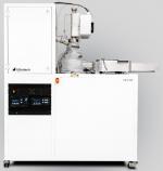
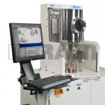
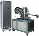 PHI VersaProbe III AD Scanning XPS Microprobe PHI VersaProbe III AD Scanning XPS Microprobe
The core technology of the VersaProbe III AD is PHI’s patented, monochromatic, micro-focused, scanning x-ray source which provides excellent large area and superior micro-area spectroscopy performance.
Features:
-
Air protection vessel: enabling sample workflow from glovebox to XPS directly.
-
Multi-point mode: automated high throughput scan on multiple positions/samples.
-
Micro area approach: in situ x-ray imaging at high spatial resolution (<10 µm) for elemental and chemical state analysis, including mapping and line profile.
-
Thin film profile analysis: using Ar ion, or C60 cluster gun with minimized chemical state damage.
-
Angle resolved XPS (non-destructive): thickness and composition analysis of ultra-thin films.
-
UPS: valence band structure and work function measurement using low energy UV source (He I: 21.2 eV and He II: 40.8 eV).
Manufacturer product page
|
|
|

Oxford Cypher ES Eviromental AFM
The Asylum Research Cypher ES provides full environmental control with high resolution, speed, and stability. It operates in controlled gas or liquid environments at temperatures from 0–250 °C, including some of the harshest chemical environments.
Features:
-
BlueDrive™ simplifies tapping mode and improves stability and quantitative performance by driving the cantilever with blue-laser excitation.
-
Sealed environmental cell with temperature control enables gas and liquid perfusion and supports biological samples. Heating and Cooling 0–120°C to minimize thermal drift. Heating to 250 °C enables wide-range temperature control.
-
Multiple measurement modes supported:
Tapping mode imaging
Contact mode imaging
Force curves and force mapping
Piezoresponse force microscopy (PFM): lithography and mapping
Conductive AFM (C-AFM): conductivity mapping with contact AFM
…
Manufacturer product page
|
|
|
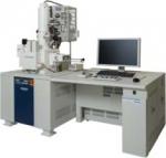
Hitachi SU8230 UHR Cold Field Emission (CFE) SEM
Hitachi’s next generation Cold Field Emission SEM offers unmatched low‑voltage imaging and comprehensive analytical microanalysis with the uncompromised performance of CFE.
Features:
-
High image resolution: 0.8 nm.
-
Air protection vessel: enabling the workflow from glovebox to SEM directly.
-
EDS (horizontal insert): ~10-100 times high signal sensitivity than tilted model; Featured with 10 – 100 nm mapping resolution with higher sensitivity to light element detection.
-
Deceleration mode (0.1-1 kV): enhanced surface details and high resolution on 2D materials.
-
STEM: scanning TEM capability.
-
External BSE (photodiode backscattered electron) horizontal insert detector.
|
|
|
Rigaku SmartLab X-ray Diffractometer
The SmartLab X-ray Diffraction System includes a highly stable and reliable sealed tube x-ray generator that is fully integrated within the automated diffraction system and is compatible with the full range of SmartLab goniometer configurations.
Features:
-
Auto sampler stage (10 samples): automated high throughput scans.
-
High temperature attachment: in situ temperature (<1500 ºC) dependent scans in air, vacuum or inert gas (argon and helium).
-
Air protection vessel: enabling sample workflow from glovebox to XRD.
-
Micro size sample analysis.
-
Thin film analysis: stress test, GI XRD, rock curve, In-plane diffraction, etc.
|
Raman Spectroscopy
|
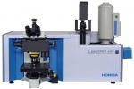
Horiba LabRAM HR Evolution
Horiba LabRAM HR Evolution systems are designed for both micro- and macro-scale measurements, delivering advanced confocal imaging in 2D and 3D. The true confocal microscope enables highly detailed images and reliable analysis—quickly and with confidence.
Features:
-
Multi-laser capability: Options include 532 nm and 633 nm laser sources.
-
True confocal microscopy: Objective choices include 10×, 50×, and 100× (air), 60× (liquid), and 50× long working distance (LWD).
-
Ultra-fast Raman imaging: Powered by SWIFT™ and DuoScan™ technologies.
-
Automation and flexibility: A fully automated, adaptable platform that supports in situ measurements with 3D-designed containers.
Manufacturer product page
|
Physical Property Measurement System (PPMS)
|
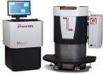 Quantum Design PPMS® DynaCool™ Quantum Design PPMS® DynaCool™
The instrument uses a single two-stage Pulse Tube cooler to cool the superconducting magnet and the samples under study, providing a low vibration environment for electronic measurements. It employs a unique He-4 -based gas flow control system providing rapid temperature cycling and accurate temperature control. It also comes standard with an integrated Cryopump used to pump out the sample space to a vacuum of < 10-4 Torr.
Features:
-
Temperature range: 0.3 K – 400 K
-
Magnetic field: ±14 Tesla.
-
Electrical Transport Option (ETO): AC Resistance measurements (frequency range: 0.1 – 200 Hz), Hall Effect, I-V sweeps. Measurement sensitivity: a few nV; resistance range: a few μΩ to GΩ.
-
Vibrating Sample Magnetometer (VSM): measuring static (DC) magnetic moment as a function of temperature or field. Can take small single crystals, thin films (can be oriented with applied field in- or out-of film plane), sintered polycrystalline pieces and loose powders.
|
|
|
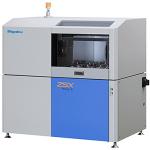
Rigaku ZSX Primus II XRF Spectrometer
The ZSX Primus II with its tube-above optics is a fully automated, sequential WDXRF spectrometer incorporating a smaller footprint and the most advanced design in the WDXRF industry. The tube-above optics of the ZSX Primus II, coupled with the ultra-thin end-window Rh target X-ray tube, guarantees reliability, flexibility and ease of use. Micro Analysis, down to 500 microns, and Mapping is now a field upgradeable option.
Features:
-
Wavelength Dispersive X-ray Fluorescence (WDXRF): high spectral resolution (typically 5 – 20 eV) with minimal spectral overlaps.
-
Measurement range: Be to U.
-
Tube above optics: minimizes contamination issues.
-
Micro analysis: analyze samples as small as 500 µm.
-
Mapping: obtain elemental topography/distribution.
|
BET Surface Area and Porosity Analysis (affiliated with Energy Sciences Institute)
|
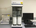 Micromeritics ASAP 2460 Surface Area and Porosity Analyzer Micromeritics ASAP 2460 Surface Area and Porosity Analyzer
The instrument incorporates a unique expandable system designed for high-performance and high sample throughput. It also includes intuitive MicroActive software that combines user-defined reports with the ability to interactively evaluate isotherm
Features:
-
Fully automated modular system optimized for walk-up sample screening.
-
High throughput with two independent analysis stations.
-
BET surface area measurements in as little as 30 minutes.
-
Pore-size range from 0.35 nm to 300 nm; Surface-area capability up to several thousand m2/g.
-
Innovative MicroActive software with advanced NLDFT modeling.
|
Thin Film Deposition Systems (affiliated with Energy Sciences Institute)
|
FijiTM 200 Gen 2
Plasma Atomic Layer Deposition System
Features:
- Continuous Mode™ (Traditional Thermal ALD)
- Exposure Mode™ (High Aspect Ratio ALD)
- Plasma Mode™ (Plasma-Enhanced ALD)
- Substrate Size: up to 200 mm
- Substrate Temperature: 500°C 200 mm substrate heater standard; 800°C 100 mm substrate heater optional
- Deposition Uniformity: 1σ Uniformities; Thermal Al2O3 – 1.5% Plasma Al2O3 – 1.5%
- Precursors: 4 precursor lines standard; 6 precursor lines optional; Accommodates gas, liquid, or solid precursors; Individually heatable to 200°C
- Gases: 100 sccm Ar precursor carrier gas MFC; 200 sccm Ar plasma gas MFC; 100sccm N2 plasma gas MFC; 100 sccm O2 plasma gas MFC; 100 sccm H2 plasma gas MFC
Manufacturer product page
|
MB-EcoVap Thin Film Coater (MBRAUN)
Features:
- For substrates up to 70 x 70 mm or 100 mm wafers
- Automatic chamber lifting mechanism
- Shielded view port for visual process monitoring
- Recipe programmable PLC control
- Removable protective shielding
- Compatible with most standard deposition sources
- Ergonomic to operate, easy to clean
- UL listed and CE compliant
Manufacturer product page
|